


About Us
Executive Editor:Publishing house "Academy of Natural History"
Editorial Board:
Asgarov S. (Azerbaijan), Alakbarov M. (Azerbaijan), Aliev Z. (Azerbaijan), Babayev N. (Uzbekistan), Chiladze G. (Georgia), Datskovsky I. (Israel), Garbuz I. (Moldova), Gleizer S. (Germany), Ershina A. (Kazakhstan), Kobzev D. (Switzerland), Kohl O. (Germany), Ktshanyan M. (Armenia), Lande D. (Ukraine), Ledvanov M. (Russia), Makats V. (Ukraine), Miletic L. (Serbia), Moskovkin V. (Ukraine), Murzagaliyeva A. (Kazakhstan), Novikov A. (Ukraine), Rahimov R. (Uzbekistan), Romanchuk A. (Ukraine), Shamshiev B. (Kyrgyzstan), Usheva M. (Bulgaria), Vasileva M. (Bulgar).


Engineering
 PDF
PDFAbstract. Perovskite solar cells have numerous advantages such as high optical absorption, band gap tunability, light weight, low cost and easy solution processed fabrication at low temperature on large area flexible substrates. This work addresses inverted heterostructure of perovskite solar cells (PSCs). This heterostructure is composed of FTO/PEDOT−PSS/Perovskite/PCBM/CdS/Ag. The fabricated PSCs exhibit PCE of 1.01% for the proposed sample structure. PEDOT-PSS is used to increase the efficiency of the perovskite solar cell at ambient conditions. Furthermore, we used Cadmium Sulphide (CdS) as an electron transport layer (ETL) along with PCBM for the first time in inverted PSCs. The utilization of CdS as an ETL enhanced the reflection of light back towards absorbing layer which effectively increases the generation of excitons. Atomic force microscopy (AFM) images are utilized to study the surface morphology of various interfacial layers. To study the crystal structure of the perovskite layer X-ray diffraction graphs have been taken. Further, to find the absorption spectra of the device UV-Visible spectroscopy has been done.
Keywords: Perovskite, Cadmium Sulphide, rectification ratio, saturation current, Electron transport layer, Solar Cell.
1 Introduction
Recently, organometallic halide perovskite have proved to be efficient materials for high performance nanostructure devices [1-5]. Perovskite family have shown efficient results in light emitting diodes, field effect transistors, photo detectors and sensors [6]. In solar cells, the power conversion efficiency of lead halide perovskite based devices has increased from 3.8% to more than 20% [7-10]. Perovskite solar cells (PSCs) can be fabricated by using different approaches including low cast and low temperature solution process [9-11]. In a typical perovskite heterojunction solar cell, perovskite act as light absorbing layer sandwiched between electron transport layer (ETL) and hole transport layer (HTL) [12-15].
In spite having good PCE, PSCs having stability issues as these devices degraded rapidly compare to other types of solar cells which is a big hurdle in its commercial applications. The major cause of this issue can be a poor interface between interfacial layers and with substrate. In PSCs Poly(3,4-ethylene-dioxythiophene):poly(4-styrenesulfonate) (PEDOT:PSS) is most oftenly used as HTL in due to its high work function, good conductivity and easy solution processing technique [15-17]. Another layer deposited on perovskite is the ETL that must consist of material having (HOMO) level below the valance band of perovskite. Most often this position has been dominated by fullerene derivative, [6, 6]-phenyl C61-butyric acid methyl ester (PCBM), as ETL.
This work addresses perovskite based inverted hetrojunction solar cell. The aim of this work is to introduce new ETL and HTL for inverted structure. For this purpose, two perovskite based solar cells are fabricate having FTO/PEDOT-PSS/Perovskite/PCBM/Cds/Ag. PEDOT-PSS is used as an HTL to increase the stability of perovskite layer and to improve charge transport rate. Whereas CdS is introduced as a new ETL for the first time in inverted perovskite solar cell in combination with PCBM to increase hole blocking and reflection of light back towards light absorbing layer which ultimately enhance the device performance. [18-19]
2 Experimental work
Perovskite (CH3NH3PbI3-XClX), Cadmium Sulphide (CdS), Fullerene derivative [6, 6]-phenyl-C61-butyric acid methyl ester (PCBM) and Poly (3, 4-ethylenedioxythiophene) −Poly (styrenesulfonate) (PEDOT−PSS) were purchased from Ossila and FTO coated glass was used as a substrate.
The fabrication of solar cells was carried out in open air environment at room temperature with relative Humidity greater than 40%. Before fabrication of device we isolated FTO layer form the sides of glass to avoid short-circuiting between top and bottom electrodes. Following this, the substrates were cleaned sequentially in detergent, deionized water, acetone and isopropyl alcohol for 10 minutes. The substrates were then heated on hot plate at 120ºC for 30 minutes. The first deposited layer is PEDOT−PSS act as hole transport layer. PEDOT−PSS was spin coated on FTO coated glass at 2000 rpm for 30 sec and annealed at temperature of 130ºC for 10 minutes. Perovskite layer was spin coated on PEDOT-PSS at 3000 rpm for 30 sec and chlorobenzene was also dropped on perovskite during last 15 seconds. After this sample was annealed on hot plate at 100ºC for 90 minutes. During the annealing process the color of perovskite layer changed from pale yellow to dark brown which confirms the formation of perovskite layer. Fullerene derivative [6, 6]-phenyl-C61-butyric acid methyl ester (PCBM) act as an ETL. The solution of PCBM was prepared in chlorobenzene with concentration of 20 mg/ml. PCBM was spin coated on perovskite layer at 1500 rpm for 30 sec. CdS was also used as additional ETL which was deposited on PCBM by using vacuum thermal evaporator. A 70 nm thick CdS layer was deposited at pressure of at 10-6 mbar. For top contacts we used metal electrodes deposited by thermal evaporation of silver at a pressure of 10-6 mbar. The complete process of device fabrication is schematically depicted in Fig 1.
3 Results and Discussion
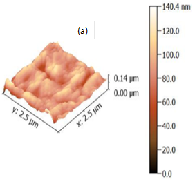
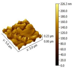
AFM images are used to examine the surface morphology of interfacial layers taken by Flex AFM Nanosurf 3000. Figure 2 (a) shows the AFM images of PEDOT−PSS layer at 2.5µm. It can be seen that film is well covered, well adherent and uniform, however, not free from crystal defects. The AFM images of perovskite at 5.0 µm are demonstrated in Figure 2 (b) which reveals good morphology and coverage of the film. The AFM images for perovskite layer spin coated on PDOT-PSS shows that the film is well covered and uniform but not free from crystal defects. Moreover, the large grain size indicates roughness of the film causes increase in series resistance which may results in degradation in the device performance.
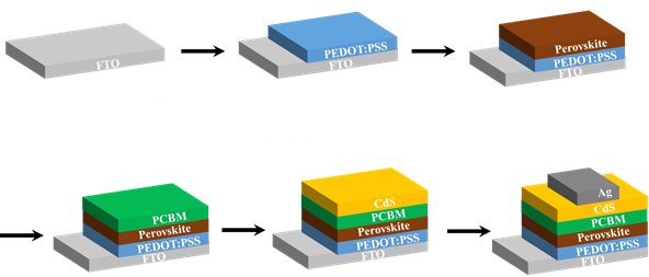
Fig.1 schematic view of layer by layer fabrication procedure of inverted perovskite solar cell.
 .
.
Fig.2 (a) Atomic force microscopy (AFM) image of PEDOT−PSS at 2.5µm on glass substrate (b) AFM images of Perovskite layer spin coated on PEDOT−PSS at 5.0 µm.
XRD technique is used to identify the material and its degree of crystallinity. In case of composite structures, it is very helpful to know about the composition of materials used in that particular structure. To study the crystal structure of perovskite (CH3NH3PbI3-XClX), XRD technique is used. Figure 3(a) shows the XRD spectra of perovskite layer. The peaks are observed at 28.4º and 43.1º representing (220) and (330) planes of cubic crystal. UV-Visible spectroscopy is used to study the absorption spectrum of material in ultraviolet and visible region of light. Figure 3(b) illustrates the absorption spectrum of methyl halide perovskite used in this experiment. It can be observed that absorption of light take place in a broad spectrum from 350 nm to 750 nm. This indicates that perovskite is most suitable material for photovoltaic application. 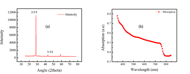
Fig.3 (a) X-ray diffraction pattern of perovskite (CH3NH3PbI3-XClX) spin coated on FTO coated glass substrate, (b) UV-Visible absorption spectrum of perovskite layer.
We performed electrical characterization of our devices to calculate different parameters of the solar cell. The current voltage characteristics were studied by using keithly source meter 2420. The J-V characteristics of PSCs under dark condition are demonstrated in Fig 4 (a) & (b). It can be observed that the devices exhibit diode-like behavior. To study this behavior under dark condition, forward and reverse biased currents are analyzed. Due to majority carrier current increases faster in forward biasing compare to reverse biasing. This confirm the formation of active junction at interfaces of perovskite with hole and electron transport layers. Therefore rectifying behavior of the junction have been achieved.
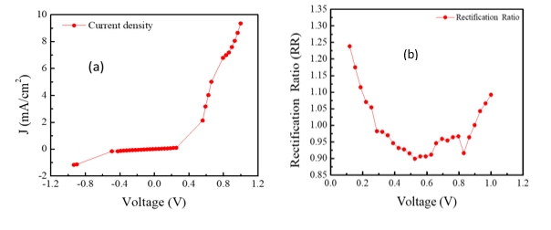
Fig.4 (a) J-V curves measurement of perovskite solar Cell under dark condition (b) Rectification ratio vs applied voltage (RR-V) plot for FTO/PEDOT−PSS/Perovskite/PCBM/CdS/Ag photovoltaic cell.
The Rectification ratio RR can be estimated from Figure 4 (a) for all the devices by using equation,
 (4.1)
(4.1)
Here, RR is the rectification ratio,  is forward biased current and
  is reverse biased current. As rectification ratio depends upon applied voltage, the graph for rectification ratio at different voltages for all four devices is demonstrated in Fig 4 (b) . Saturation current of the devices can be measured from J-V curves under dark conditions. Shockley equation for ideal diode under dark condition is given by
 (4.2)
(4.2)
Where,  is current density,
  is saturation current density, q is electronic charge, V is applied voltage, k is the Boltzmann constant and T is temperature in Kelvin. In the above equation, if applied voltage is few millivolts then -1 is negligible, so the intersection of l
 -Vcurve at V=0 gives value of saturation current density. Figure 5 shows l-V curves for both devices. The value of saturation current is 0.00094 mA.
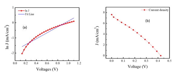
Fig.5 (a) LnI-V plot for FTO/PEDOT−PSS/Perovskite/PCBM/CdS/Ag photovoltaic cell (b) J-V curves for PSC illuminated at standard A.M 1.5 and irradiance of 100mW/cm2.
The J-V curves for the proposed device structure under illumination of 100mW/cm2 is demonstrated in Figure 5 (b). By using this curve, we calculated the solar cell parameters like short circuit current density ( ), open circuit voltage (
 ), Fill factor (FF), Maximum power point (MPP) and power conversion efficiency (η). The FF is estimated by using following equation.
 (4.1)
(4.1)
Here  and
and  are current density and voltage at maximum power point, respectively.
The efficiency is then calculated by using the relation:
 (4.2)
(4.2)
For this device,  of 9.52 mA/cm2,
  of 0.52V and FF of 0.29 is achieved. The PCE for this device is calculated to be 1.01%. The series and shunt resistance of the device is also calculated. Series resistance (RS) and shunt resistance (Rsh) is 922Ω and 1379Ω respectively. The high value of series resistance results in decrease of PCE of both the devices.
4 Conclusion
In summary, we have fabricated solution processed inverted PSCs at room temperature in high humidity conditions. Device has the structure of FTO/PEDOT−PSS/Perovskite/PCBM/CdS/Ag. CdS was used as an ETL for the first time in inverted PSC along with PCBM to increase the reflection of light back towards active layer. Moreover, we incorporated PEDOT−PSS as a HTL. The perovskite layer deposited on PEDOT−PSS is non-homogeneous and less dense due to acidic nature of PEDOT−PSS. The J-V measurements of the devices were performed under light and dark condition. This device structure exhibit a PCE of 1.01%. Efficiency of the device can be improved by replicating this work in nitrogen and controlled environment, also the decrease in thickness of the layers can improve PCE of the device.
Acknowledgements
We wish to acknowledge Faculty of Engineering Sciences and Faculty of Electronic Engineering, GIK Institute for the support extended to this work. We are also thankful to Pakistan council of renewable energy technology (PCRET) for their cooperation.
2. A. Kojima, K. Teshima, Y. Shirai, and T. Miyasaka, "Organometal halide perovskites as visible-light sensitizers for photovoltaic cells," Journal of the American Chemical Society, vol. 131, pp. 6050-6051, 2009.
3. H.-S. Kim, C.-R. Lee, J.-H. Im, K.-B. Lee, T. Moehl, A. Marchioro, et al., "Lead iodide perovskite sensitized all-solid-state submicron thin film mesoscopic solar cell with efficiency exceeding 9%," Scientific reports, vol. 2, p. 591, 2012.
4. J. H. Noh, S. H. Im, J. H. Heo, T. N. Mandal, and S. I. Seok, "Chemical management for colorful, efficient, and stable inorganic-organic hybrid nanostructured solar cells," Nano letters, vol. 13, pp. 1764-1769, 2013.
5. M. Liu, M. B. Johnston, and H. J. Snaith, "Efficient planar heterojunction perovskite solar cells by vapour deposition," Nature, vol. 501, pp. 395-398, 2013.
6. D. B. Mitzi, "Synthesis, structure, and properties of organic?inorganic perovskites and related materials," Progress in Inorganic Chemistry, Volume 48, pp. 1-121, 2007.
7. B. V. Lotsch, "New light on an old story: perovskites go solar," Angewandte Chemie International Edition, vol. 53, pp. 635-637, 2014.
8. N.-G. Park, "Organometal perovskite light absorbers toward a 20% efficiency low-cost solid-state mesoscopic solar cell," The Journal of Physical Chemistry Letters, vol. 4, pp. 2423-2429, 2013.
9. H. J. Snaith, "Perovskites: the emergence of a new era for low-cost, high-efficiency solar cells," The Journal of Physical Chemistry Letters, vol. 4, pp. 3623-3630, 2013.
10. I. Grinberg, D. V. West, M. Torres, G. Gou, D. M. Stein, L. Wu, et al., "Perovskite oxides for visible-light-absorbing ferroelectric and photovoltaic materials," Nature, vol. 503, pp. 509-512, 2013.
11. S. Kazim, M. K. Nazeeruddin, M. Gr?tzel, and S. Ahmad, "Perovskite as light harvester: a game changer in photovoltaics," Angewandte Chemie International Edition, vol. 53, pp. 2812-2824, 2014.
12. J. Burschka, N. Pellet, S.-J. Moon, R. Humphry-Baker, P. Gao, M. K. Nazeeruddin, et al., "Sequential deposition as a route to high-performance perovskite-sensitized solar cells," Nature, vol. 499, pp. 316-319, 2013.
13. N. J. Jeon, J. H. Noh, W. S. Yang, Y. C. Kim, S. Ryu, J. Seo, et al., "Compositional engineering of perovskite materials for high-performance solar cells," Nature, vol. 517, pp. 476-480, 2015.
14. P. Docampo, F. C. Hanusch, S. D. Stranks, M. D?blinger, J. M. Feckl, M. Ehrensperger, et al., "Solution deposition?conversion for planar heterojunction mixed halide perovskite solar cells," Advanced Energy Materials, vol. 4, 2014.
15. G. E. Eperon, V. M. Burlakov, P. Docampo, A. Goriely, and H. J. Snaith, "Morphological control for high performance, solution?processed planar heterojunction perovskite solar cells," Advanced Functional Materials, vol. 24, pp. 151-157, 2014.
16. D. Liu and T. L. Kelly, "Perovskite solar cells with a planar heterojunction structure prepared using room-temperature solution processing techniques," Nature photonics, vol. 8, pp. 133-138, 2014.
17. A. Mei, X. Li, L. Liu, Z. Ku, T. Liu, Y. Rong, et al., "A hole-conductor-free, fully printable mesoscopic perovskite solar cell with high stability," Science, vol. 345, pp. 295-298, 2014.
18. S. Ananthakumar, J. R. Kumar, and S. M. Babu, "Cesium lead halide (CsPbX3, X Cl, Br, I) perovskite quantum dots-synthesis, properties, and applications: a review of their present status," Journal of Photonics for Energy, vol. 42001, p. 1, 2016.
19. Z. Song, S. C. Watthage, A. B. Phillips, and M. J. Heben, "Pathways toward high-performance perovskite solar cells: review of recent advances in organo-metal halide perovskites for photovoltaic applications," Journal of Photonics for Energy, vol. 6, p. 022001, 2016.
Tahseen Amin Khan Qasuriaa, Shahid Alama, Nabeel Anwar Qureshi FABRICATION OF INVERTED PEROVSKITE SOLAR CELL WITH CADMIUM SULPHIDE AS ELECTRON TRANSPORT LAYER. International Journal Of Applied And Fundamental Research. – 2018. – № 3 –
URL: www.science-sd.com/475-25393 (02.07.2026).